Your new post is loading...
The development of efficient organic light-emitting diodes (OLED) and organic photovoltaic cells requires control over the dynamics of spin sensitive excitations. A team of scientists have developed a plastic-like polymer that emits white light more efficiently than current organic LEDs. In recent years household lighting has moved from the incandescent light bulb to the compact fluorescent, and more recently to LEDs. But to create white light manufacturers cluster red, green and blue LEDs, or use blue LED light, some of which is converted to yellow, and then mixing the two colours to create white light. Organic light emitting diodes (OLEDs) use polymer chains that glow when they are stimulated with an electrical current or light. However, current OLED displays also combine red, blue and green to create white light. Professor Valy Vardeny of the University of Utah and colleagues have combined polymer chains with heavy atoms to create a new type of OLED that they believe could create white light much more simply. "This new polymer has all those colours simultaneously, so there is no need for small pixels and complicated engineering to create them," says Vardeny. Polymers have two kinds of electronic states - single and triplet. When the polymer is stimulated, the singlet state emits blue light. The triplet state, which can emit lower energy red light, is much harder to stimulate. If a heavy atom such as iridium, platinum or palladium is incorporated into the polymer chain, this triplet state is easier to stimulate. "The idea is to incorporate the heavy atom into the chain so that you don't have to rely on mixtures or energy transfers. The compound itself contains all the ingredients," says Vardeny. Varying how often platinum appears in the chain allows the researchers to 'tune' the light it emits. For example, a platinum atom after each 'unit' in the chain emits violet and yellow light, while a platinum atom after every third unit results in blue and orange light.
Periodic structures that control photons, much as semiconductors control electrons, came into being in the late 1980s, through a complex interchange between experiment and theory. Photonic crystals, structures that allow researchers to manipulate the passage of electromagnetic radiation, went from theoretical possibility to experimental reality over a period of several years. Two papers inPhysical Review Letters, in 1987 and 1991, stand as bookends to the emergence of these new structures. Since then, researchers have used photonic materials to guide light in devices such as fiber optics and have also realized that such materials exist in nature, for example in the scales that give butterfly wings their iridescent colors. The picture above shows a 3D structure made of plastic is the first photonic crystal ever made, with a forbidden frequency band in the microwave range. Holes are 6 millimeters across (only a small portion of the crystal is shown). In the 1980s, Eli Yablonovitch, then at Bell Communications Research (now part of Ericsson) in Red Bank, New Jersey, was worried about losses in semiconductor lasers and other devices arising from light emitted at unwanted frequencies. In a 1987 paper in Physical Review Letters he observed that these losses would not occur in a medium that prevented these frequencies of light from propagating. He proposed that such a medium could be made by carving out voids in a transparent material to create a periodic structure, analogous to a crystal lattice, with the material and the voids having different indices of refraction (different speeds of light). Yablonovitch offered an analogy to semiconductors, which have an energy “band gap” between the valence electrons—associated with chemical bonds—and the conduction electrons. Just as electrons with energies in the band gap cannot exist in a semiconductor, so light with frequencies in the electromagnetic band gap would not exist in the proposed structure. In each case, the periodic structure leads to destructive wave interference (electron waves or electromagnetic fields) that leads to the gap. It happened that Sajeev John of Princeton University independently made a related proposal at the same time. Yablonovitch, now at the University of California, Berkeley, says that he and John met to discuss their ideas and decided to use the words “photonic crystal” to describe structures with band gaps for electromagnetic waves. In trying to make a photonic crystal, Yablonovitch worked with microwaves, rather than visible or infrared light, because their longer wavelengths allowed him to develop periodic designs with spacings on the scale of a few millimeters. In 1989, after testing many different possibilities, he and T. J. Gmitter published what they claimed to be the first structure with a photonic band gap, consisting of spherical holes arrayed throughout a block of plastic in a face-centered cubic (fcc) pattern. Both Yablonovitch and John favored such structures, thinking that because the fcc pattern is close to isotropic, it ought to block radiation in all directions, and the measurements seemed to agree. Spurred by this paper, theorists worked out how to apply Maxwell’s equations to photonic structures. However, three analyses of the Yablonovitch-Gmitter structure indicated that it had only a “pseudogap,” meaning that the forbidden frequency range shrank to zero for certain directions of radiation. That was a shock, says Yablonovitch, but he realized that his measurements had not been comprehensive enough. Building a structure with an omni-directional band gap took another two years. In their 1991 paper, Yablonovitch and Gmitter were joined by one of the theorists who had criticized their earlier work, K. Ming Leung of Polytechnic University (now Polytechnic Institute of New York University). The team described a structure that, according to both experiment and theory, possessed a true photonic band gap—one that prevented radiation in all directions. To create the structure, the team drilled a series of holes through a solid block of plastic. Starting with a triangular array of target points on the top surface, they drilled three holes at each point, each time angling the bit at 35° from vertical but rotating horizontally to get three equally-spaced directions as seen from above. The pattern turned out to be a variety of fcc related to the crystal structure of diamond, which was suggested by one of the earlier theoretical analyses to possess a true band gap. The team got the widest band gap when the hole diameter was so large that the drilled-out volume amounted to 78% of the total structure. Although it was several more years before the first photonic crystal for optical wavelengths was made, Yablonovitch regards his 1987 paper as the beginning of photonic crystals. John Joannopoulos of the Massachusetts Institute of Technology agrees that the paper was important for “throwing out an idea,” although it offered no proof of the concept. Ironically, he says, it was the erroneous 1989 structure that got more attention and caused the theorists to jump in, which led to the first true photonic band gap. In recent years, photonic crystals have been used for several purposes, such as optical fibers that in some cases confine light more effectively than traditional fibers
MIT researchers discover a new phenomenon that could lead to new types of lasers and sensors. There are several ways to “trap” a beam of light — usually with mirrors, other reflective surfaces, or high-tech materials such as photonic crystals. But now researchers at MIT have discovered a new method to trap light that could find a wide variety of applications.
The new system, devised through computer modeling and then demonstrated experimentally, pits light waves against light waves: It sets up two waves that have the same wavelength, but exactly opposite phases — where one wave has a peak, the other has a trough — so that the waves cancel each other out. Meanwhile, light of other wavelengths (or colors) can pass through freely.
The researchers say that this phenomenon could apply to any type of wave: sound waves, radio waves, electrons (whose behavior can be described by wave equations), and even waves in water.
“For many optical devices you want to build,” Soljačić says — including lasers, solar cells and fiber optics — “you need a way to confine light.” This has most often been accomplished using mirrors of various kinds, including both traditional mirrors and more advanced dielectric mirrors, as well as exotic photonic crystals and devices that rely on a phenomenon called Anderson localization. In all of these cases, light’s passage is blocked: In physics terminology, there are no “permitted” states for the light to continue on its path, so it is forced into a reflection.
In the new system, however, that is not the case. Instead, light of a particular wavelength is blocked by destructive interference from other waves that are precisely out of phase. “It’s a very different way of confining light,” Soljačić says.
While there may ultimately be practical applications, at this point the team is focused on its discovery of a new, unexpected phenomenon. “New physical phenomena often enable new applications,” Hsu says. Possible applications, he suggests, could include large-area lasers and chemical or biological sensors.
The researchers first saw the possibility of this phenomenon through numerical simulations; the prediction was then verified experimentally.
In mathematical terms, the new phenomenon — where one frequency of light is trapped while other nearby frequencies are not — is an example of an “embedded eigenvalue.” This had been described as a theoretical possibility by the mathematician and computational pioneer John von Neumann in 1929. While physicists have since been interested in the possibility of such an effect, nobody had previously seen this phenomenon in practice, except for special cases involving symmetry.
This work is “very significant, because it represents a new kind of mirror which, in principle, has perfect reflectivity,” says A. Douglas Stone, a professor of physics at Yale University who was not involved in this research. The finding, he says, “is surprising because it was believed that photonic crystal surfaces still obeyed the usual laws of refraction and reflection,” but in this case they do not.
Stone adds, “This is in fact a realization of the famous ‘bound state in the continuum’ proposed by von Neumann and [theoretical physicist and mathematician Eugene] Wigner at the dawn of quantum theory, but in a practical, realizable form. The potential applications the authors mention, to high-power single-mode lasers and to large-area chemical [and] biological sensing, are very intriguing and exciting if they pan out.”
Using nanostructured glass, scientists at the University of Southampton have, for the first time, experimentally demonstrated the recording and retrieval processes of five dimensional digital data by femtosecond laser writing. The storage allows unprecedented parameters including 360 TB/disc data capacity, thermal stability up to 1000°C and practically unlimited lifetime.
Coined as the 'Superman' memory crystal, as the glass memory has been compared to the "memory crystals" used in the Superman films, the data is recorded via self-assembled nanostructures created in fused quartz, which is able to store vast quantities of data for over a million years. The information encoding is realised in five dimensions: the size and orientation in addition to the three dimensional position of these nanostructures.
A 300 kb digital copy of a text file was successfully recorded in 5D using ultrafast laser, producing extremely short and intense pulses of light. The file is written in three layers of nanostructured dots separated by five micrometers. The self-assembled nanostructures change the way light travels through glass, modifying polarisation of light that can then be read by combination of optical microscope and a polariser, similar to that found in Polaroid sunglasses.
The research is led by the ORC researcher Jingyu Zhang and conducted under a joint project with Eindhoven University of Technology. "We are developing a very stable and safe form of portable memory using glass, which could be highly useful for organisations with big archives. At the moment companies have to back up their archives every five to ten years because hard-drive memory has a relatively short lifespan," says Jingyu. "Museums who want to preserve information or places like the national archives where they have huge numbers of documents, would really benefit." The Physical Optics group from the ORC presented their ground-breaking paper at the photonics industry's renowned Conference on Lasers and Electro-Optics (CLEO'13) in San Jose. The paper, '5D Data Storage by Ultrafast Laser Nanostructuring in Glass' was presented by the during CLEO's prestigious post deadline session. Professor Peter Kazansky, the ORC's group supervisor, adds: "It is thrilling to think that we have created the first document which will likely survive the human race. This technology can secure the last evidence of civilisation: all we've learnt will not be forgotten."
The team are now looking for industry partners to commercialise this ground-breaking new technology.
A single cell in our body is composed of thousands of millions of different biomolecules that work together in an extremely well-coordinated way. Likewise, many biological and biochemical reactions occur only if molecules are present at very high concentrations. Understanding how all these molecules interact with each other is key to advancing our knowledge in molecular and cell biology. This knowledge is of central and fundamental importance in the quest for the detection of the earliest stages of many human diseases. As such, one of ultimate goals in Life Sciences and Biotechnology is to observe how individual molecules work and interact with each other in these very crowded environments. Unfortunately, detecting one molecule amongst millions of neighbouring molecules has been technically impossible until now. The key to successfully detecting the single molecule lies in the conception and production of a working device that shrinks the observation region to a tiny size that is comparable to the size of the molecule itself, i.e. only a few nanometres. Researchers at the Fresnel Institute in Marseille and ICFO-the Institute for Photonic Sciences in Barcelona report in Nature Nanotechnology the design and fabrication of the smallest optical device, capable of detecting and sensing individual biomolecules at concentrations that are similar to those found in the cellular context. The device called "antenna-in-a-box" consists on a tiny dimer antenna made out of two gold semi-spheres, separated from each other by a gap as small as 15nm. Light sent to this antenna is enormously amplified in the gap region where the actual detection of the biomolecule of interest occurs. Because amplification of the light is confined to the dimensions of the gap, only molecules present in this tiny region are detected. A second trick that the researchers used to make this device work was to embed the dimer antennas inside boxes also of nanometric dimensions. "The box screens out the unwanted "noise" of millions of other surrounding molecules, reducing the background and improving as a whole the detection of individual biomolecules.", explains Jerome Wenger from Fresnel Institute. When tested under different sample concentrations, this novel antenna-in-box device allowed for 1100-fold fluorescence brightness enhancement together with detection volumes down to 58 zeptoliters (1 zL = 10E-21L), i.e., the smallest observation volume in the world. The antenna-in-a-box offers a highly efficient platform for performing a multitude of nanoscale biochemical assessments with single molecule sensitivity at physiological conditions. It could be used for ultrasensitive sensing of minute amounts of molecules, becoming an excellent early diagnosis device for biosensing of many disease markers. "It can also be used as an ultra-bright optical nanosource to illuminate molecular processes in living cells and ultimately visualize how individual biomolecules interact with each other. This brings us closer to the long awaited dream of biologists", concludes ICFO researcher Prof. Maria Garcia-Parajo.
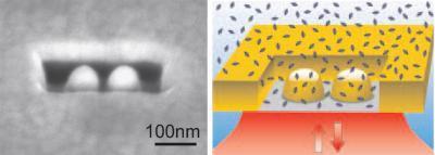
Since the 1970s, physicists have used laser beams to trap and study small objects, from cells down to individual atoms. More recently, researchers have developed multilaser systems that can manipulate many particles at once. But these systems are large and complex, so they have limited applications. Now, scientists have developed a simple system that uses a single laser beam to direct hundreds of particles at one time to assemble into two-dimensional structures (Nano Lett., DOI: 10.1021/nl400918x). This compact optical trap could eventually help researchers make materials for new types of sensors, optical devices, and chemical filters. In optical traps, a concentrated beam of light puts a force on particles, causing them to move toward the most intense part of the beam. Current systems that can manipulate many particles at once do so by generating complex light fields using space-hogging setups with many lenses. Michelle Povinelli, an electrical engineer at theUniversity of Southern California, wanted to develop a simple system for generating these complex light fields. She envisioned one that was small enough to fit on a chip. That way, researchers could readily integrate the traps into devices like photonic circuits or chemical sensors, making them more amenable to applications. Povinelli’s optical trap uses a patterned slab of silicon called a photonic crystal. She and her collaborators etched into the crystal a regular array of 300-nm-diameter holes, spaced 860 nm from one another. They immersed the slab in a suspension of 520-nm-diameter polystyrene particles and illuminated it from below with a laser. The particles floating above the crystal then moved into the holes, forming a square crystal lattice measuring 13 μm on each side. Paul V. Braun, a materials scientist at the University of Illinois, Urbana-Champaign, says that compared with other optical traps, the USC device offers simplicity and easy integration with other devices. But the existing systems can hold particles in different configurations, while the photonic crystal requires them to stay in a fixed pattern dictated by the pattern of holes. So the devices are easy to make but aren’t as flexible as current optical traps, he says. Povinelli says she is now working out how to design photonic crystals that can switch the particles between different configurations when she changes the wavelength of laser light.
A research team at the University of Southampton in England has built a fiber cable that is capable of carrying data at 99.7 percent of the vacuum-speed of light. They have done so, they report in their paper published in the journal Nature Photonics, by constructing a cable with a hollow core and special inner walls that prevent refraction.
Fiber cables technically at least, carry data at the speed of light (299,792,458 meters per second in a vacuum), because the media they carry, is in fact a beam of light. But, in practice, data is carried far slower than that because of latency delays caused by refraction as light moves through the silica glass, which reduces common fiber cable data rate throughput by approximately 31 percent. To get around this problem, researchers have been looking at ways to replace the core of the fibers with air, which suffers far less from refraction.
The stumbling point has been how to get the light beams moving through the cables to follow the cable when bends and turns are encountered. That's where this new research comes in—the group has found a new way to build a hollow core fiber cable that allows for bending light as it moves around turns while minimizing loss due to refraction. The secret is, the team reports, an "ultra-thin photonic-bandgap rim" that provides low data loss, a wide bandwidth and far less latency than standard fiber cables. The result is a cable that in the lab was able to move data, using division multiplexing, at a rate of 73.7 terabits per second, which is approximately 1000 times better than standard fiber cable.
There is a hitch, of course. While data loss is relatively low (3.5 dB/km), it's still too high for use with anything but very short-hop applications, such as the fiber connections inside of supercomputers or perhaps within a data center where the paths the fiber cables take can be run in extremely straight lines. Because of that, the researchers will be working to improve their cable—if they succeed it could one day mean the end of waiting when downloading files, or better yet, to making applications such as real-time ultra high definition 3D transmissions, possible for general use across the Internet.
Novel multicore fiber design enables 10E15 bits per second. Optical communications and IT services provider NEC Corp. of America and fiber developerCorning Inc., have announced what they are calling “record-breaking results in transmission capacity over optical fibers”. The result was first reported at the OSA’s Frontiers in Optics/Laser Science XXVIII (FiO/LS) meeting, held in October 2012. The partners commented, “As the foundation of telecommunications networks, optical fiber innovation enables carriers to cost effectively keep up with ever-growing traffic demands.” Researchers from the NEC Labs in Princeton, NJ, USA, and from Corning’s Sullivan Park Research Center in Corning, NY, successfully demonstrated ultra-high speed transmission with a capacity of 1.05 petabit/s (1015 bits per second) over novel multi-core fiber that contains 12 single-mode and two few-mode cores by employing the advanced space division multiplexing scheme and optical multiple-input multiple-output signal processing technique.
Ultrafast, efficient, and reliable single-photon detectors are among the most sought-after components in photonics and quantum communication, which have not yet reached maturity for practical application. Physicist Dr. Wolfram Pernice of the Karlsruhe Institute of Technology (KIT), in cooperation with colleagues at Yale University, Boston University, and Moscow State Pedagogical University, achieved the decisive breakthrough by integrating single-photon detectors with nanophotonic chips. The detector combines near-unity detection efficiency with high timing resolution and has a very low error rate. Without reliable detection of single photons, it is impossible to make real use of the latest advances in optical data transmission or quantum computation; it is like having no analog-digital converter in a conventional computer to determine whether the applied voltage stands for 0 or 1. Although a number of different single-photon detector models have been developed over the past few years, thus far, none have provided satisfactory performance. Several new ideas and advanced developments went into the prototype developed within the "Integrated Quantum Photonics" project at the DFG Center of Functional Nanostructures (CFN). The new single-photon detector, tested in the telecommunications wavelength range, achieves a previously unattained detection efficiency of 91%. The detector was realized by fabricating superconducting nanowires directly on top of a nanophotonic waveguide. This geometry can be compared to a tube that conducts light, around which a wire in a superconducting state is wound and, as such, has no electric resistivity. The nanometer-sized wire made of niobium nitride absorbs photons that propagate along the waveguide. When a photon is absorbed, superconductivity is lost, which is detected as an electric signal. The longer the tube, the higher is the detection probability. The lengths involved are in the micrometer range. A special feature of the detector is its direct installation on the chip, which allows for it to be replicated at random. The single-photon detectors built thus far were stand-alone units, which were connected to chips with optical fibers. Arrangements of that type suffer from photons being lost in the fiber connection or being absorbed in other ways. These loss channels do not exist in the detector that is now fully embedded in a silicon photonic circuit. In addition to high detection efficiency, this gives rise to a remarkably low dark count rate. Dark counts arise when a photon is detected erroneously: for instance, because of a spontaneous emission, an alpha particle, or a spurious field. The new design also provides ultrashort timing jitter of 18 picoseconds, which is 18 times 10^-12 seconds. The novel solution also makes it possible to integrate several hundreds of these detectors on a single chip. This is a basic precondition for future use in optical quantum computers. The detector demonstrated in this study was designed to work at wavelengths in the Telekom bandwidth. The same detector architecture can also be used for wavelengths in the range of visible light. This would allow the principle to be employed in analyses of all structures that emit little light, i.e., photons, such as single molecules or bacteria.
Researchers have demonstrated a new technology that combines a laser and electric fields to create tiny centrifuge-like whirlpools to separate particles and microbes by size, a potential lab-on-a-chip system for medicine and research. The theory behind the technology, called rapid electrokinetic patterning - or REP - has been described in technical papers published between 2008 and 2011. Now the researchers have used the method for the first time to collect microscopic bacteria and fungi, saidSteven T. Wereley, a Purdue University professor of mechanical engineering. The technology could bring innovative sensors and analytical devices for lab-on-a-chip applications, or miniature instruments that perform measurements normally requiring large laboratory equipment. REP is a potential new tool for applications including medical diagnostics; testing food, water and contaminated soil; isolating DNA for gene sequencing; crime-scene forensics; and pharmaceutical manufacturing. "The new results demonstrate that REP can be used to sort biological particles but also that the technique is a powerful tool for development of a high-performance on-chip bioassay system," Wereley said. The technology works by using a highly focused infrared laser to heat fluid in a microchannel containing particles or bacteria. An electric field is applied, combining with the laser's heating action to circulate the fluid in a "microfluidic vortex," whirling mini-maelstroms one-tenth the width of a human hair that work like a centrifuge to isolate specific types of particles based on size. Here the rapid electrokinetic patterning technique is used to arrange bacteria into a specific pattern. The technique may be used as a tool for nanomanufacturing because it shows promise for the assembly of suspended particles, called colloids. The ability to construct objects with colloids makes it possible to create structures with particular mechanical and thermal characteristics to manufacture electronic devices and tiny mechanical parts. Particles of different sizes can be isolated by changing the electrical frequency, and the vortex moves wherever the laser is pointed, representing a method for positioning specific types of particles for detection and analysis.
Now anybody can pick up and move micron-scale particles using their hands and arms thanks to a Kinect-controlled infrared holographic laser device called HoloHands. The interface allows user to “pick up” and “push” particles they see on a computer screen using hand, arm and body movements alone. The system shows users the field of view in which the tweezers operate. A wave of the hand creates a trapping region, which holds particles. This can then be picked up and moved with further arms movements. It may also be possible to build stuff by hand using a Lego-like set up where students make microscale devices and machines using HoloHands.
Photons, in the form of optical pulses, radio waves, and the like, have been used to transmit data for decades. The next phase will probably involve using the quantum states of the photons themselves to carry information. In terms of these quantum states, photons possess two distinct polarization orientations, along with a theoretically infinite number of helical wave forms, in which the photons rotate around the direction they're moving. The latter have garnered a lot of interest, as they could potentially carry a lot more data than other optical methods. Possible applications include quantum computing, improved fiber optic communication, point-to-point data transfer across free space, and microscopy. Researchers have now developed a way to produce twisted light beams using silicon chips, the starting point for compact, efficient optical communication. Xinlun Cai and colleagues shaped photons using a microscopic, ring-shaped grating, which sent twisted light out in a specified pattern. Each ring was small enough to be fabricated into integrated circuits, and capable of emitting multiple vortexes of light simultaneously. The same type of chip could also serve as a receiver for twisted light, and manipulate waves that transit through it. Photons possess a number of quantum properties that can be used to encode information. You can think of photon polarization as like the rotation of a planet on its axis. In this view, the helical shape of the light wave—known as its orbital angular momentum (OAM)—is akin to the planet's orbit around the Sun. These properties are independent of each other, and of the wavelength of light, so they can be manipulated separately. Whereas polarization occurs as a combination of two possible orientations, the OAM theoretically can have infinite values, though in practice far fewer states are available. Nevertheless, exploiting OAM greatly expands the potentially exploitable quantum states of photons we could put to use. This is an exciting step toward OAM-based devices. The researchers showed how simple microscale ring-shaped chambers fabricated from silicon could produce any number of possible helical waveforms, opening up many possible channels for future investigation.
NTT and three partners demonstrated ultra-large capacity transmission of 1 petabit (1000 terabit) per second over a 52.4 km length of 12-core (light paths) optical fiber.
The present achievement indicates that transmission of one petabit per second (Pbps), capacity equivalent to sending 5,000 HDTV videos of two hours in a single second is possible over 50 km, which is approximately the distance between medium-haul telecom offices. This sets a new world record throughput over a single strand of optical fiber.
This remarkable achievement was reported as a postdeadline paper*1 on September 20, 2012 at the European Conference and Exhibition on Optical Communications (ECOC 2012), the largest conference on optical communication in Europe, that was held in Amsterdam, the Netherlands, from September 16-20, 2012.
This work was partially based on work commissioned by the National Institute of Information and Communications Technology (NICT).
|
A pair of breakthroughs in the field of silicon photonics by researchers at the University of Colorado Boulder, the Massachusetts Institute of Technology and Micron Technology Inc. could allow for the trajectory of exponential improvement in microprocessors that began nearly half a century ago—known as Moore's Law—to continue well into the future, allowing for increasingly faster electronics, from supercomputers to laptops to smartphones.
The research team, led by CU-Boulder researcher Milos Popovic, an assistant professor of electrical, computer and energy engineering, developed a new technique that allows microprocessors to use light, instead of electrical wires, to communicate with transistors on a single chip, a system that could lead to extremely energy-efficient computing and a continued skyrocketing of computing speed into the future. Popovic and his colleagues created two different optical modulators—structures that detect electrical signals and translate them into optical waves—that can be fabricated within the same processes already used in industry to create today's state-of-the-art electronic microprocessors. The modulators are described in a recent issue of the journal Optics Letters. First laid out in 1965, Moore's Law predicted that the size of the transistors used in microprocessors could be shrunk by half about every two years for the same production cost, allowing twice as many transistors to be placed on the same-sized silicon chip. The net effect would be a doubling of computing speed every couple of years. The projection has held true until relatively recently. While transistors continue to get smaller, halving their size today no longer leads to a doubling of computing speed. That's because the limiting factor in microelectronics is now the power that's needed to keep the microprocessors running. The vast amount of electricity required to flip on and off tiny, densely packed transistors causes excessive heat buildup. "The transistors will keep shrinking and they'll be able to continue giving you more and more computing performance," Popovic said. "But in order to be able to actually take advantage of that you need to enable energy-efficient communication links."
Photonics as a field began with the invention of the laser in 1960. Photonics includes the generation, emission, transmission, modulation, signal processing, switching, amplification, and detection/sensing of light. Photonics covers all technical applications of light over the whole spectrum from ultraviolet over the visible to the near-, mid- and far-infrared. Most applications, however, are in the range of the visible and near infrared light. The term photonics developed as an outgrowth of the first practical semiconductor light emitters invented in the early 1960s and optical fibers developed in the 1970s.
Using carpets of aligned carbon nanotubes, researchers from Rice University and Sandia National Laboratories have created a solid-state electronic device that is hardwired to detect polarized light across a broad swath of the visible and infrared spectrum. “Detecting polarized light is extremely useful,” said Rice’s Junichiro Kono, professor of electrical and computer engineering and of physics and astronomy. “Many animals and insects can see polarized light and use it for navigation, communication and more. Humans can’t see polarized light, so we rely on devices to do that for us.” Most devices can’t detect polarized light directly. Instead, engineers place a grate or filter in front of the detector. “Our photodetector discerns polarized light intrinsically, much like the photoreceptors in the eyes of animals and insects that see polarized light,” said François Léonard at Sandia National Laboratories, one of the lead researchers on the study. Polarized light consists of individual electromagnetic waves oscillating parallel to one another. The effect is created when light reflects from a transparent material, which is why polarized sunglasses reduce the glare from water, glass and other surfaces. Astronomers use polarized light in a number of ways, and there are a number of applications for polarimetry in communications and the military. Rice’s new photodetector is the latest development from a collaboration between Rice and Sandia under Sandia’s National Institute for Nano Engineering program, which is funded by the Department of Energy. In February, Kono, Léonard and colleagues described a new method for making photodetectors from carpets of carbon nanotubes — long, narrow tubes of pure carbon that are about as wide as a strand of DNA. The nanotube carpets used in the photodetectors are grown in the lab of Rice chemist Robert Hauge, who pioneered a process for growing densely packed nanotubes on flat surfaces. Xiaowei He, a graduate student in Kono’s group, found a way to use Teflon film to flatten these tightly packed nanotubes so that they are aligned in the same direction. Each carpet contains dozens of varieties of nanotubes, and about two-thirds of the varieties are semiconductors. Because each of the semiconducting varieties interacts with a specific wavelength of light, Kono’s team was able to show in its earlier work that the flattened, aligned carpets of nanotubes could serve as broad-spectrum photodetectors.
Researchers at MIT have proposed a new system that combines ferroelectric materials — the kind often used for data storage — with graphene, a two-dimensional form of carbon known for its exceptional electronic and mechanical properties. The resulting hybrid technology could eventually lead to computer and data-storage chips that pack more components in a given area and are faster and less power-hungry.
The new system works by controlling waves called surface plasmons. These waves are oscillations of electrons confined at interfaces between materials; in the new system the waves operate at terahertz frequencies. Such frequencies lie between those of far-infrared light and microwave radio transmissions, and are considered ideal for next-generation computing devices.
The team’s new system allows waves to be concentrated at much smaller length scales, which could lead to a tenfold gain in the density of components that could be placed in a given area of a chip, Fang says.
The team’s initial proof-of-concept device uses a small piece of graphene sandwiched between two layers of the ferroelectric material to make simple, switchable plasmonic waveguides. This work used lithium niobate, but many other such materials could be used, the researchers say.
Light can be confined in these waveguides down to one part in a few hundreds of the free-space wavelength, Jin says, which represents an order-of-magnitude improvement over any comparable waveguide system. “This opens up exciting areas for transmitting and processing optical signals,” he says.
Rice University scientists have unveiled a robust new method for arranging metal nanoparticles in geometric patterns that can act as optical processors that transform incoming light signals into output of a different color. Rice's team used the method to create an optical device in which incoming light could be directly controlled with light via a process known as "four-wave mixing." Four-wave mixing has been widely studied, but Rice's disc-patterning method is the first that can produce materials that are tailored to perform four-wave mixing with a wide range of colored inputs and outputs. "Versatility is one of the advantages of this process," said study co-author Naomi Halas, director of LANP and Rice's Stanley C. Moore Professor in Electrical and Computer Engineering and a professor of biomedical engineering, chemistry, physics and astronomy. "It allows us to mix colors in a very general way. That means not only can we send in beams of two different colors and get out a third color, but we can fine-tune the arrangements to create devices that are tailored to accept or produce a broad spectrum of colors." The information processing that takes place inside today's computers, smartphones and tablets is electronic. Each of the billions of transistors in a computer chip uses electrical inputs to act upon and modify the electrical signals passing through it. Processing information with light instead of electricity could allow for computers that are both faster and more energy-efficient, but building an optical computer is complicated by the quantum rules that light obeys.
Researchers at University of California, Santa Barbara, in collaboration with colleagues at the École Polytechnique in France, have conclusively identified Auger recombination as the mechanism that causes light emitting diodes (LEDs) to be less efficient at high drive currents.
Until now, scientists had only theorized the cause behind the phenomenon known as LED “droop”—a mysterious drop in the light produced when a higher current is applied. The cost per lumen of LEDs has held the technology back as a viable replacement for incandescent bulbs for all-purpose commercial and residential lighting.
This could all change now that the cause of LED efficiency droop has been explained, according to researchers James Speck and Claude Weisbuch of the Center for Energy Efficient Materials at UCSB, an Energy Frontier Research Center sponsored by the U.S. Department of Energy.
Knowledge gained from this study is expected to result in new ways to design LEDs that will have significantly higher light emission efficiencies. LEDs have enormous potential for providing long-lived high quality efficient sources of lighting for residential and commercial applications. The U.S. Department of Energy recently estimated that the widespread replacement of incandescent and fluorescent lights by LEDs in the U.S. could save electricity equal to the total output of fifty 1GW power plants.
“Rising to this potential has been contingent upon solving the puzzle of LED efficiency droop,” commented Speck, professor of Materials and the Seoul Optodevice Chair in Solid State Lighting at UCSB. “These findings will enable us to design LEDs that minimize the non-radiative recombination and produce higher light output.”
A new type of material that halts and absorbs light may lead to advances in solar energy, stealth technology, and other fields, experts report. Researchers ath the University at Buffalo developed a “hyperbolic metamaterial waveguide” that halts and ultimately absorbs each frequency of light, at slightly different places in a vertical direction, to catch a “rainbow” of wavelengths. The technology is essentially an advanced microchip made of ultra-thin films of metal and semiconductors and/or insulators. “Electromagnetic absorbers have been studied for many years, especially for military radar systems,” says Qiaoqiang Gan, an assistant professor of electrical engineering at University at Buffalo. “Right now, researchers are developing compact light absorbers based on optically thick semiconductors or carbon nanotubes. However, it is still challenging to realize the perfect absorber in ultra-thin films with tunable absorption band. “We are developing ultra-thin films that will slow the light and therefore allow much more efficient absorption, which will address the long existing challenge.” Light is made of photons that, because they move extremely fast, are difficult to tame. In their initial attempts to slow light, researchers relied upon cryogenic gases, which are very cold—roughly 240 degrees below zero Fahrenheit—and difficult to work with outside a laboratory. Gan previously helped pioneer a way to slow light without cryogenic gases. He and other researchers at Lehigh University made nanoscale-sized grooves in metallic surfaces at different depths, a process that altered the optical properties of the metal. While the grooves worked, they had limitations. For example, the energy of the incident light cannot be transferred onto the metal surface efficiently, which hampered its use for practical applications. Researchers say the technology could lead to advancements in an array of fields. For example, in electronics there is a phenomenon known as crosstalk, in which a signal transmitted on one circuit or channel creates an undesired effect in another circuit or channel. The on-chip absorber could potentially prevent this. The on-chip absorber may also be applied to solar panels and other energy-harvesting devices. It could be especially useful in mid-infrared spectral regions as thermal absorber for devices that recycle heat after sundown, Gan says. Technology such as the stealth bomber involves materials that make planes, ships, and other devices invisible to radar, infrared, sonar, and other detection methods. Because the on-chip absorber has the potential to absorb different wavelengths at a multitude of frequencies, it could be useful as a stealth-coating material.
African physicists build the first laser with a beam that can be controlled and shaped digitally. Physicists currently change the shape by placing various kinds of beam-shaping devices in front of the laser. These include lenses, mirrors and digital holograms generated using spatial light modulators. But because these devices are essentially bolted on to the front of a laser, they all require expensive custom optics that have to be calibrated each time they are changed. Today, however, Sandile Ngcobo at the University of KwaZulu–Natal in South Africa and few buddies, say they’ve worked out a way round this. And they’ve designed and built a device to test their idea. The solution is simple. Instead of putting a spatial light modulator in front of the laser, they’ve built one in to the device, where it acts as the mirror at one end of the cavity. In this way, the spatial light modulator shapes the beam as it is being amplified. The result is that the beam is already shaped in the required way when it emerges from the laser cavity. “We have demonstrated a novel digital laser that allows arbitrary intra-cavity laser beam shaping to be executed on the fly,” say Ngcobo and co. The big advantage of all this is that the spatial light modulator generates patterns electronically. That allows these guys to change the beam shape at the touch of a button and without any of the time-consuming set up required with other methods. They call their device a digital laser, because the beam can be shaped electronically with a computer. That’s the first time such a machine has been built. The results are interesting. In putting the digital laser though it’s paces, they’ve shown how it can produce all kinds of beams with different shapes (see figure). The applications are many. It will make various kinds of technologies much simpler, such as holographic laser tweezers and controlling aberrations in real time. Impressive stuff!
If you want to create a moving light source, you have a few possibilities. One is to mount a light emitter in some kind of mechanical housing—the approach used in, say, theatrical spotlights, which stagehands swivel and tilt to track performers. Another possibility, however, is to create an array of light emitters and vary their "phase"—the alignment of the light waves they produce. The out-of-phase light waves interfere with one another, reinforcing each other in some directions but annihilating each other in others. The result is a light source that doesn't move, but can project a beam in any direction. Such "phased arrays" have been around for more than a century, used most commonly in radar transmitters, which can be as much as 100 feet tall. But in this week's issue of Nature, researchers from MIT's Research Laboratory of Electronics (RLE) describe a 4,096-emitter array that fits on a single silicon chip. Chips that can steer beams of light could enable a wide range of applications, including cheaper, more efficient, and smaller laser rangefinders; medical-imaging devices that can be threaded through tiny blood vessels; and even holographic televisions that emit different information when seen from different viewing angles. In their Nature paper, the MIT authors—Michael Watts, an associate professor of electrical engineering, Jie Sun, a graduate student in Watts' lab and first author on the paper, Sun's fellow graduate students Erman Timurdogan and Ami Yaacobi, and Ehsan Shah Hosseini, an RLE postdoc—report on two new chips. Both chips take in laser light and re-emit it via tiny antennas etched into the chip surface.
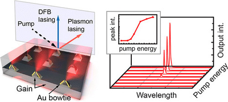
A Northwestern University research team has found a way to manufacture single laser devices that are the size of a virus particle and that operate at room temperature. These plasmonic nanolasers could be readily integrated into silicon-based photonic devices, all-optical circuits and nanoscale biosensors. Reducing the size of photonic and electronic elements is critical for ultra-fast data processing and ultra-dense information storage. The miniaturization of a key, workhorse instrument -- the laser -- is no exception.
A new theory and simulations have been developed that describe a spinning optical soliton whose propagation spontaneously excites knotted and linked optical vortices. The nonlinear phase of the self-trapped light beam breaks the wave front into a sequence of optical vortex loops around the soliton, which, through the soliton's orbital angular momentum and spatial twist, tangle on propagation to form links and knots. Similar spontaneous knot topology should be a universal feature of waves whose phase front is twisted and nonlinearly modulated, including superfluids and trapped matter waves.
Using lasers, researchers were able to take control of Caenorhabditis elegans — tiny, transparent worms — by manipulating neurons in the worms’ brain and instruct it to turn in any direction they chose. They implanted false sensory information, fooling the worm into thinking food was nearby. By taking control of such complex behaviors, researchers hope to understand how a worm's nervous system functions. The work is important because, by taking control of complex behaviors in a relatively simple animal — C. elegans have just 302 neurons — researchers can understand how its nervous system functions. The hairy goal is to activate only one neuron, which is challenging because the animal is moving quickly, and the neurons are densely packed near its head, so the challenge is to acquire an image of the animal, process that image, identify the neuron, track the animal, position your laser, and shoot the particular neuron — and do it all in 20 milliseconds, or about 50 times a second. The system that researchers eventually developed uses a movable table to keep the crawling worm centered beneath a camera and laser. The system was not only capable of controlling the worms’ behavior, but their senses as well. In one test, the researchers were able to trick a worm’s brain into believing food was nearby, causing it to make a beeline toward the imaginary meal. “By manipulating the neural system of this animal, we can make it turn left, we can make it turn right, we can make it go in a loop, we can make it think there is food nearby,” the principal investigator Ramanathan said. “We want to understand the brain of this animal, which has only a few hundred neurons, completely, and essentially turn it into a video game, where we can control all of its behaviors.”
|